DOC #1 · EDGE AI COMPUTATIONEdge AI & Diagnostics
Thirty Use Cases, No Accelerator
50 MHz RV32IM edge AI compute envelope, 19 lightweight models, fixed-point DSP pipeline & CWRU audit
Formal proof that high-accuracy industrial condition monitoring and predictive diagnostics do not require heavy transformer acceleration or multi-watt NPU arrays. By exploiting the architectural inversion that comparisons and table lookups cost almost nothing on an integer CPU, tree ensembles achieve parity with deep learning (95.6% vs 97–100% on CWRU bearing benchmarks) while requiring zero multiplications and running 50–500× faster.
Compute Engine50 MHz RV32IM (Zero NPU)
Scalar Ceiling12.5 MMAC/s (int8)
RAM Ceiling16.5 KB SRAM budget
Standard ComplianceISO 13373 / 20816 / 20958
Key architectural proofs- 12.5 MMAC/s integer budget leaves 82% CPU headroom at 10 kHz FOC current loop rate
- Single-bin Goertzel DFT replaces multi-megabyte FFT buffers for broken rotor bar detection
- Documents non-monotonic Kurtosis trap: kurtosis drops as spall rounds over, requiring RMS cross-checking
- Uncovers critical 100% synthetic accuracy leakage in academic CWRU bearing benchmark datasets
DOC #7 · SKU BLUEPRINTProduct Portfolio
SKU Blueprint, October 2026 (11 SKUs + D100)
The source of record for every SKU on this site. One handout per SKU: what it replaces, market, share needed, unit economics, buyers, policy driver, process choice and the FPGA-to-chip boundary
The current product portfolio. Each SKU is a standalone handout answering the same nine questions: what the part is, what it replaces, how big the market is, what share is needed and whether that is realistic, what each unit earns, who buys it, the policy driver, why this process node, and where the FPGA prototype ends and the chip begins. Adds SKU-10 DG32-Max Secure MCU and SKU-11 SOH-Aware BMS Controller to the earlier nine. Volumes, prices and shares are the company’s own estimates.
Portfolio11 SKUs plus the Track B D100 drone SoC
ProcessSkyWater 130 nm and SCL 180 nm; SKU-7 on IHP SG13G2
FormatNine questions per SKU, answered in the same order
ShuttleNine prototypes on the ChipFoundry December 2026 shuttle
Key architectural proofs- New in this edition: SKU-10 DG32-Max Secure MCU and SKU-11 SOH-Aware BMS Controller
- Each SKU states what it replaces, who buys it, the policy driver and why its process node was chosen
- Status per SKU: what is RTL-ready, simulated or FPGA-validated, and which parts take the December 2026 shuttle
- The D100 drone SoC is Track B, funded by a separate round and taking nothing from the eleven chips’ budget
DOC #3 · HARDWARE DSHOT RX RTLHigh-Speed Motor Telemetry
dgrid_dshot_rx RTL Specification
Hardware DShot receive engine, bidirectional GCR 4b→5b eRPM telemetry reply & pad-ring reuse
Complete RTL engineering specification for dgrid_dshot_rx: offloads ESC motor signal decoding and bidirectional eRPM telemetry reply entirely into deterministic hardware logic. Features glitch-free pad-ring direction reuse without external analog multiplexers, early-abort frame suppression, and floorplan trade-off recovering 4,800 µm² die area.
Data RatesDShot150 / 300 / 600 / 1200
Telemetry EngineHardware GCR 4b→5b eRPM reply
Memory BusSlot 0xC APB memory-mapped
Floorplan Area28 KB vs 32 KB SRAM layout lever
Key architectural proofs- Zero-CPU overhead motor command capture and validation up to DShot1200 rates
- Autonomous GCR 4b→5b eRPM packet assembly and transmission without software intervention
- Bidirectional GPIO pad-ring reuse with deterministic turnaround timing
- 28 KB vs 32 KB SRAM floorplan trade-off analysis for sky130 multi-project shuttle packaging
DOC #4 · DUAL-DOMAIN SOC & ATTENTIONCondition Monitoring & Attention
DG32-2DOM Architecture & Block Definition
Dual 50/114 MHz clocks, 4-phase CDC bridges, INT8 attention engine & AVIP diagnostics
System architecture of DG32-2DOM: adds an INT8 multi-head self-attention engine on an independent 114 MHz clock domain alongside the frozen 50 MHz lockstep control core. Robust 4-phase CDC bridges isolate domains so condition monitoring cannot stall the motor control loop. Utilizes AVIP stator current signature analysis to detect bearing faults with zero additional sensor BOM.
Clock Partition50 MHz Control · 114 MHz Attention
CDC Mechanism4-Phase Asynchronous Handshake
Attention CoreINT8 Multi-Head (40-bit Accumulator)
Sensorless MCSAAVIP Stator Current Bearing Analysis
Key architectural proofs- Rigorous dual-clock domain isolation: control loop worst-case execution time guaranteed untouched
- 40-bit accumulator headroom prevents INT8 softmax overflow and numerical saturation
- AVIP stator current diagnostics isolate inner/outer race bearing faults without accelerometers
- 18 on-die SRAM macros occupying 86% of sky130 active die area with positive timing slack
DOC #5 · DEFENCE & ECONOMIC STRATEGYGeopolitics & Strategic Moats
Mature-Node Silicon for India’s Defence (Whitepaper v3)
$9B mature-node import funnel, 198-day loop, 10x NRE dismantling & DAP-2020 Make-II statutory moats
The foundational 71-page master whitepaper establishing India’s mature-node semiconductor doctrine. Sizes India’s roughly $9B mature-node import funnel, and shows how open-source EDA and shared MPW shuttles bring NRE to ₹0.6–1.2 Cr per chip against $2–5M for a conventional flow, creates statutory moats through 'Boxes, Not Chips' integration under DAP-2020, and models Chinese supply disruption resilience. September 2026 edition, superseded in part by the October SKU Blueprint (chip count, clock, orders, funding). Its orders figure includes a contract this site withholds as misdescribed; do not cite it.
Import Funnel$9B Mature-Node Defence Market
Tapeout Cadence198-Day Shuttle Loop
NRE Economics₹0.6–1.2 Cr (10x NRE reduction)
Legal FrameworkDAP-2020 Make-II · PIL-1..5 · SRIJAN
Key architectural proofs- $9B mature-node import funnel prioritized across 10 critical defence semiconductor SKUs
- 198-day tapeout loop from RTL freeze to packaged silicon delivery using OpenLane EDA
- Statutory moats under DAP-2020 Make-II and Ministry of Defence positive indigenisation lists
- Rigorous Charlie Munger inversion audits and strict stop-rules S1–S4
DOC #6 · DATASHEETS & PINOUTPackaging, Clocks & Electrical Rules
Preliminary Engineering Datasheets & Package Pinout
64-pin QFN 9×9mm pin mapping, 100% LITE/2DOM compatibility, supply sequencing & ROM boot
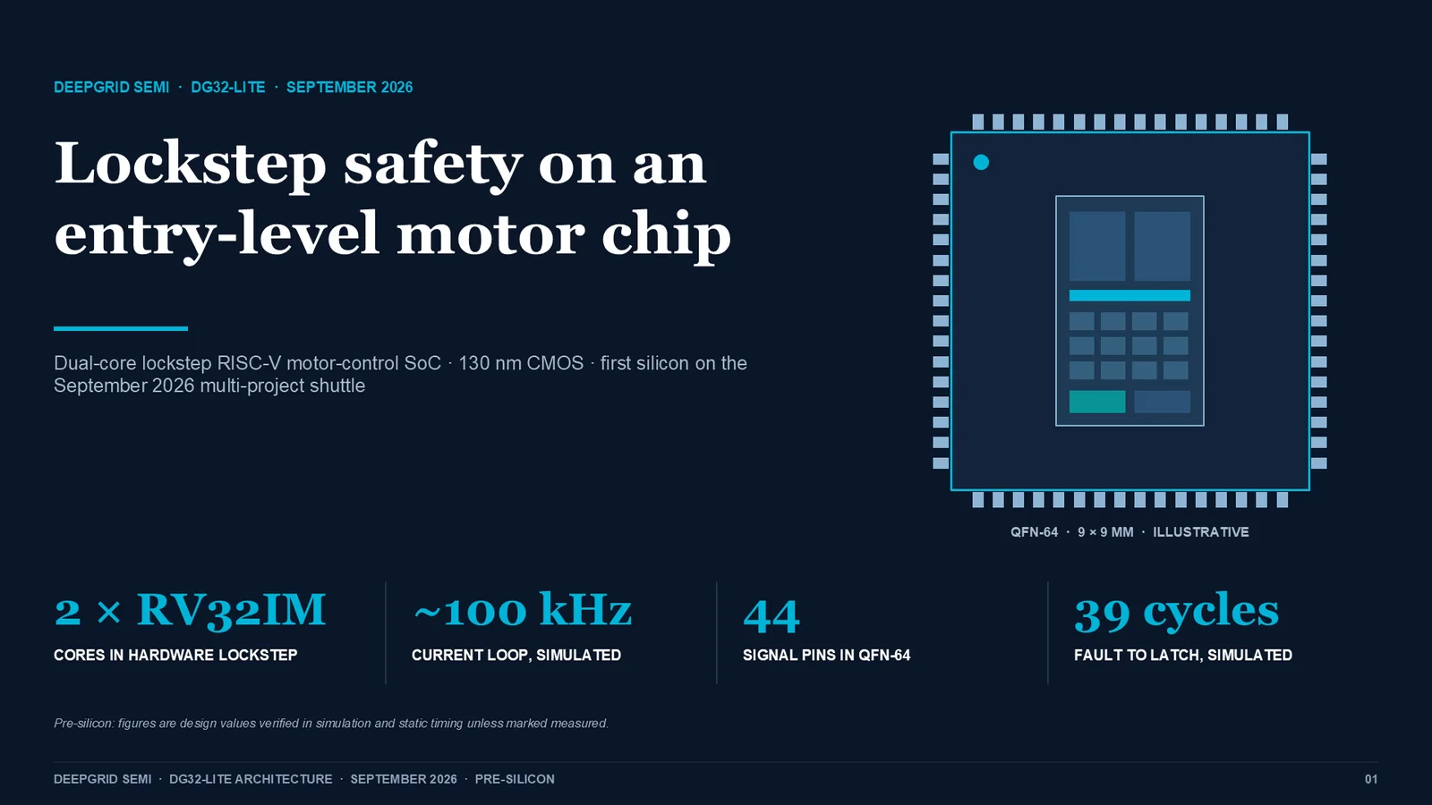
Preliminary engineering datasheet for DG32-LITE and DG32-2DOM in QFN-64. The two chips share one pinout: DG32-2DOM is a pin-compatible drop-in for DG32-LITE boards. Mandates strict power supply sequencing (3.3V I/O must lead 1.8V core by ≥1 ms to protect ESD rail diodes), defines 64 KB mask boot ROM operations, and maps all 44 signal pins.
Package SpecQFN-64 (9×9 mm, 0.5 mm pitch)
Signal Pins44 Signal Pins across 11 groups
Supply Rails1.8V Core · 3.3V I/O (Sequenced)
CompatibilityIdentical pinout (LITE & 2DOM)
Key architectural proofs- Identical 64-pin footprint allows one PCB layout to take either DG32-LITE or DG32-2DOM
- Strict power supply sequencing protects internal ESD rail clamps from latch-up breakdown
- 44 functional signal pins organized into 11 functional clusters with dedicated return paths
- 64 KB autonomous boot ROM with flash header validation and fallback UART monitor
PLATFORM · D100 DRONE SOCTactical Drone Flight Systems
D100 Tactical Drone Platform Architecture
Flight control, visual navigation and optional AI on one 28 nm chip, with an isolated hardware failsafe island
Heterogeneous multi-core SoC for tactical unmanned aerial systems. Partitions flight compute into high-performance vision/navigation (Quad RV64) and hard real-time flight control (Quad RV32), backed by a physically isolated hardware failsafe island that takes over motor control upon main OS hang or communication loss.
Process28 nm; failsafe island buildable at 130 nm
Failsafe DomainIsolated hardware failsafe island
Flight controlLockstep RISC-V pair on a DO-254 path
FundingTrack B: separate round after mature-node revenue
Key architectural proofs- Hardware failsafe island executes emergency return-to-launch (RTL) independent of Linux host
- 8 hardware-timed DShot motor channels with microsecond-level synchronization
- Direct hardware cryptographic authentication for secure datalinks
- Sub-watt low-power standby modes for extended loiter missions
PLATFORM · SDV ZONAL E/EAutomotive Zonal Controllers
DG SDV Software-Defined Vehicle Zonal Architecture
Distributed zonal controllers eliminating vehicle wire harness mass and latency
Automotive zonal E/E reference architecture replacing complex point-to-point body harnesses with 4 distributed zonal gateways. SKU-9, the zonal gateway, carries the zonal I/O: Gigabit TSN Ethernet, CAN-XL and 16 smart e-fuses in place of electromechanical relays, with software updates centralised.
Power switching16 × smart e-fuses (48 V / 12 V)
Vehicle bus4 × CAN-XL, up to 20 Mbps
Zone Clusters4 × Zonal Controllers
Safety targetISO 26262 ASIL-D (target, not certified)
Key architectural proofs- Gigabit TSN Ethernet and CAN-XL in place of electromechanical relays and point-to-point wiring
- Deterministic CAN-XL and 10BASE-T1S automotive Ethernet backbones
- Local hardware motor control and current sensing for high-reliability body actuators
- Hardware fault confinement designed to the ISO 26262 ASIL-D target
STRATEGY · SOVEREIGN SILICONManufacturing & Fab Strategy
Three-Factory Sovereign Silicon Architecture
Strategic manufacturing arbitrage across SkyWater, SCL Mohali, and Dholera 28nm fabs
Geopolitical and fab-arbitrage blueprint for Indian semiconductor sovereignty. Aligns design tooling so RTL can port seamlessly between US open-access fabs (SkyWater), Indian strategic fabs (SCL Mohali 180nm), and emerging commercial mega-fabs (Tata Dholera 28nm), guaranteeing supply continuity across international supply crunches. September 2026 edition, superseded in part by the October SKU Blueprint (chip count, clock, orders, funding). Its orders figure includes a contract this site withholds as misdescribed; do not cite it.
Foundry NetworkSkyWater · SCL Mohali · Dholera 28nm
Node Distribution180nm BCD · 130nm CMOS · 28nm Planar
Supply ResilienceSanction-proof multi-foundry PDKs
Economic Model₹10 Cr Capital Efficiency
Key architectural proofs- Multi-foundry PDK portability preventing vendor lock-in to single fabs
- Zero-NRE open-source toolchain (OpenLane/Magic/KLayout) validated on test silicon
- Strategic arbitrage between high-voltage BCD (actuators) and dense CMOS (controllers)
- Proof of concept for India’s ₹10 Cr sovereign chip initiative