
SKU-4 · 130 nm CMOS DG32 safety MCU
SKU-4 runs a checker core two cycles behind and drives FAULT_N 39 cycles after a mismatch, in simulation.
Every figure on this page is a design target unless marked otherwise.
- Lockstep
- Two cores, two-cycle skew, comparator on every committed store
- Fault responseSimulated
- 39 cycles from injected fault to latched FAULT_N (DG32-LITE, simulated)
- Package (DG32-LITE)
- QFN-64, 9 × 9 mm
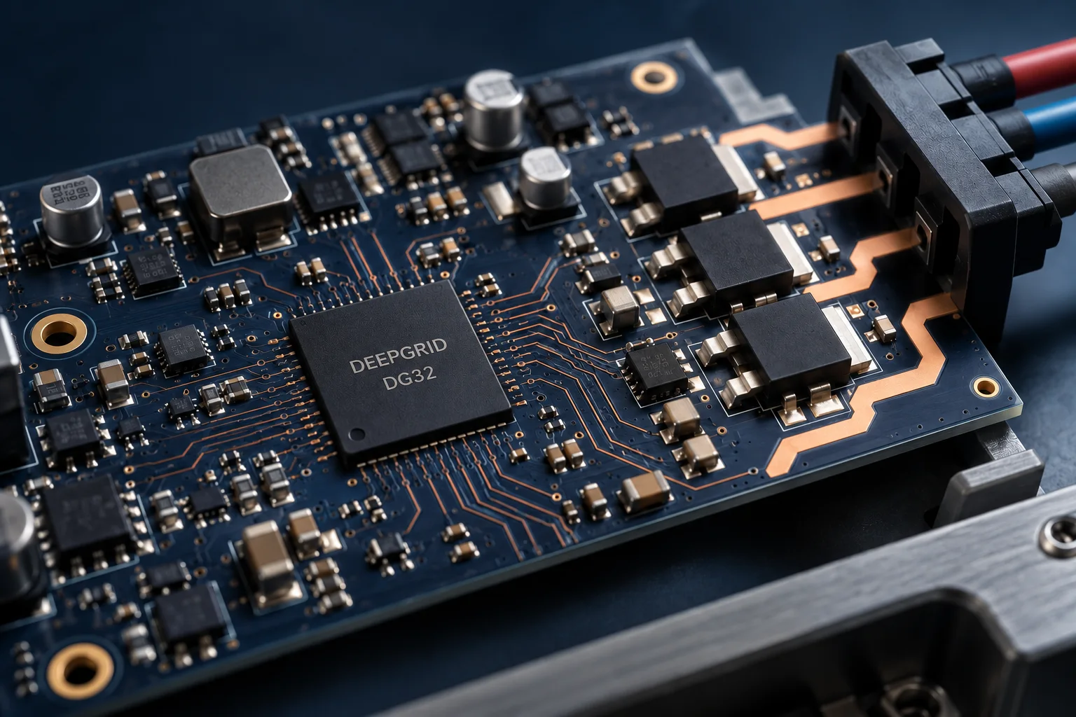
SKU-4 runs a checker core two cycles behind and drives FAULT_N 39 cycles after a mismatch, in simulation.
SKU-4 uses two processors to detect disagreement and trigger a hardware fault response. It is intended to support a system safety case.
- Job
- Make a control-core disagreement observable at the hardware fault output.
- Replaces
- Functional-safety microcontrollers of the Microchip and Renesas class.
- Status
- RTL ready; prototype on the December 2026 shuttle. Validated on FPGA at 81.25 MHz; the product is a 130 nm chip at 100 MHz.

The business case for SKU-4
Evaluate the complete response, from detecting a failure to reaching the machine’s safe state.
What it replaces
Functional-safety microcontrollers of the Microchip and Renesas class.
Customer opportunity
EV battery management, motor-safety supervision, braking and steering controllers and robot joints; and the safety processor beside SKU-1 and inside D100.
Policy and demand
The design targets the ISO 26262 ASIL-D automotive safety level; the lockstep checker has been fault-injection tested in RTL simulation.
The delivery trade-off
Running two processors costs chip area, not speed. A mature node makes that redundancy, and radiation-hardened latches, affordable.
What SKU-4 claims, what it is worth, and what gates it.
The following mechanisms explain the proposed customer benefit. Each still needs to be validated in the complete product.
SKU-4 runs a checker core two cycles behind and drives FAULT_N 39 cycles after a mismatch, in simulation.
SKU-4 uses two processors to detect disagreement and trigger a hardware fault response. It is intended to support a system safety case.
A datapath fault reaches the gate driver without firmware.
Evaluate the complete response, from detecting a failure to reaching the machine’s safe state.
39 cycles is a simulation result, not an ISO 26262 certificate.
Simulation of fault detection does not establish product certification or system-level safety.
Architecture targets, not datasheet values.
Every figure is a design target stated in the SKU Blueprint, page 19. None is a measurement of manufactured silicon.
- 39Cycles from injected fault to FAULT_NSimulated
- 2Cycles of lockstep skew
- 100 MHzProduct clock on 130 nm
Detailed architecture and specifications
- Process
- 130 nm CMOS
- Lockstep
- Two cores, two-cycle skew, comparator on every committed store
- Fault responseSimulated
- 39 cycles from injected fault to latched FAULT_N (DG32-LITE, simulated)
- Clock
- 100 MHz product on 130 nm; FPGA validation at 81.25 MHz; DG32-LITE ran at 50 MHz
- Memory
- ROM, SRAM and encrypted external flash, ECC on memory and bus; embedded-flash variant on SCL 180 nm (DG32-LITE: 64 KB ROM, 32 KB SRAM)
- Package (DG32-LITE)
- QFN-64, 9 × 9 mm
- Process
- 130 nm CMOS
- Maturity
- Pre-silicon engineering evidence
- Designed toward
- ISO 26262 ASIL-D (a path, not a certificate) · IEC 61508 SIL 3
- Source
- SKU Blueprint, October 2026, page 19
Standards the architecture is designed toward. No DeepGrid part holds a certification or qualification today.
System architecture, signal flow and engineering references
DG32-LITE is the implemented SKU-4 part, so this is its diagram: 50 MHz, boot from ROM, no on-die flash. The specification below states the SKU-4 family targets, which go beyond it.

Marker ①: The PWM fires the ADC where current ripple is lowest
3-phase PWM in Motor drive fires a sample trigger at the centre of each period, where current ripple is lowest. SAR ADC 8-bit in Sensing & math, differential at about 200 kSa/s, converts the phase current in 177 cycles. Because the converter is on the die, a sample costs a start pulse and a poll, not an external SPI read.
Motor driveSensing & math
Marker ②: CORDIC runs the transforms at a fixed, known cost
Phase current goes to CORDIC, which runs the Clarke and Park transforms with the rotor angle from Encoder + Hall, whose edge timestamps keep velocity accurate at low speed. Each CORDIC operation takes 53 to 58 cycles. The CPU core is fetch-bound at about 8 cycles per instruction, so this math stays in hardware.
Sensing & math
Marker ③: The CPU keeps only the PI regulators
The transformed currents go to MAIN core in the Safety core, which runs the d and q PI regulators in plain C. With sampling, transforms and edge generation in hardware, one loop carries about 300 cycles of fixed hardware cost. At 10 kHz on the 50 MHz clock, that leaves about 4,700 of 5,000 cycles for firmware.
Safety core
Marker ④: New duty cycles load at the next period boundary
The PI output sets the duty in shadow registers in 3-phase PWM, and the new values load at the next period boundary, so an update never lands mid-period. Timers × 2 typically hold the control-loop period and an RTOS tick. DShot × 4 shares the same pads for digital ESC frames and is selected at boot.
Motor drive
Marker ⑤: Gate signals leave for a bridge outside the package
3-phase PWM drives six gate pins, centre-aligned and complementary with programmable dead-time, to the Gate driver + 3-phase bridge outside the QFN-64 package. A hardware brake forces all six outputs off within two clock cycles and latches, so firmware can see that it happened. The power stage itself never sits on the die.
Motor drive
Marker F: A mismatch trips the bridge in 39 cycles, without firmware
CHECKER core runs the instructions of MAIN core two cycles later on the same inputs. Lockstep comparator checks every committed store; on the first mismatch, Fault latch holds the cause and drives FAULT_N low, which turns the Gate driver + 3-phase bridge off in hardware. From injected fault to latched FAULT_N took 39 cycles in simulation.
Safety core
Supervision and the bus keep every fault visible
Windowed watchdog faults a kick that arrives too early or too late, and its supply supervisor sequences reset. Interrupt controller delivers 16 sources identically to both cores, so CHECKER stays in step. On the On-chip bus, an unmapped address returns a bus error instead of a hang. Boot ROM 64 KB copies the image from QSPI NOR flash into SRAM 32 KB.
SupervisionOn-chip busMemory & boot
Numbered markers
- ①Marker ①: The PWM period centre fires the ADC sample, where current ripple is lowest.
- ②Marker ②: Phase current goes to the CORDIC, which runs the Clarke and Park transforms with the rotor angle.
- ③Marker ③: The transformed currents go to the CPU, which runs the d and q PI regulators in plain C.
- ④Marker ④: The PI output sets the PWM duty in shadow registers that load at the next period boundary.
- ⑤Marker ⑤: Gate signals leave for the external gate driver.
- FMarker F: FAULT_N from the fault latch turns the bridge off in hardware, without firmware.
Block responsibilities
- Safety core
MAIN runs the application. CHECKER runs the same instructions two cycles later on identical inputs, the comparator checks every committed store, and the fault latch holds the first cause and drives FAULT_N.
Why A silent datapath fault produces a wrong PWM edge, and a wrong edge can destroy a bridge.
Guide: Safety core- Memory and boot
The 64 KB mask ROM validates the flash image, copies it into 32 KB of dual-port SRAM and jumps to it. One SRAM port serves data, the other instruction fetch.
Why The die has no management core and no debugger halt, so the boot path must start the chip on its own.
Guide: Memory and boot- Supervision
The windowed watchdog faults a kick that arrives too early or too late. The interrupt controller delivers 16 sources identically to both cores.
Why Identical delivery is what keeps CHECKER in step when firmware branches on an interrupt or a peripheral read.
Guide: Safety core- On-chip bus
Two masters, the CPU first and the DMA second, with single-outstanding, deterministic latency. An unmapped or disabled address completes with a bus error.
Why On a chip with no debugger, a hung bus would be a brick.
Guide: Bus, system and test- Motor drive
Centre-aligned complementary PWM on six gate pins with dead-time, and a hardware brake that forces all six outputs off within two clock cycles. Four DShot channels share the PWM pads.
Why Gate timing and the safe state are too important to leave to a firmware loop.
Guide: Motor drive- Sensing and math
Encoder and Hall decode with edge timestamps, an 8-bit differential SAR ADC fired by the PWM, and a CORDIC for sin, cos and atan2 at a fixed cost per operation.
Why The CPU core is fetch-bound at about 8 cycles per instruction, so the expensive parts of the loop are hardware.
Guide: Sensing and math- Connectivity and test
Two UARTs, an SPI master, an I²C master and GPIO with atomic set and clear. JTAG and internal scan chains serve production test.
Guide: Connectivity- Off-chip
QSPI NOR flash holds the application image. The gate driver and three-phase bridge, the motor sensors and the host sit outside the package.
Guide: Power-on boot
Primary sources
- DG32-LITE architecture guideEvery block, the three data flows, timing headroom and the locked decisions.Opens in the site
- DG32-LITE preliminary datasheetPin, electrical and peripheral detail for the part.PDF · 12 pages
- DG32 QFN-64 datasheets, both partsDG32-LITE and DG32-2DOM in one document.PDF · 24 pages
- Architecture deck and narrated filmThe same diagram walked through slide by slide.Deck · film
7 integration and validation references
- Hercules safety MCUs (TI SPRY178)How a checker CPU fed the same inputs, offset by 1.5 or 2 cycles, catches faults; also why a watchdog should be windowed.Texas Instruments · PDF
- Field Orientated Control of 3-Phase AC-Motors (TI BPRA073)The Clarke and Park transforms, the PI regulator and space-vector PWM behind markers ① to ④.Texas Instruments · PDF
- The CORDIC trigonometric computing techniqueVolder, IRE Transactions on Electronic Computers, 1959: the shift-and-add method the CORDIC block uses.IEEE · DOI
- RISC-V ratified specificationsThe RV32IM instruction set both cores execute.RISC-V International
- Arm AMBA specifications, including AXIThe bus protocol family the on-chip bus and the engine bridges are modelled on.Arm
- DShot and bidirectional DShotThe digital ESC protocol the DShot channels speak.Explainer
- SkyWater SKY130 PDK documentationThe open 130 nm process the datasheet names.SkyWater · Google
Background reading explains the general technique each block uses. None of it describes this part or implies its certification.
Architecture from the SKU Blueprint, page 19. A functional view, not a floorplan.
7 questions SKU-4 has to answer before it can be relied on.
The Blueprint’s design and status notes raise these. Each is a question silicon, test or layout has to answer before SKU-4 can be relied on.
A transient that hits both cores at once must still be caught.Physics
A two-cycle skew between the cores, so the same disturbance lands on different instructions.
The fault response cannot depend on the processor that failed.Physics
The comparator, latch and fault pin are hardware; the safe state does not run through firmware.
Safety logic is small, deterministic and long-lived.Physics
A mature 130 nm CMOS process with predictable timing suits it better than a dense node.
Skewed readsOpen
How does the delay buffer make both cores see identical read data from asynchronous peripherals without stalling?
Diagnostic coverageOpen
Which built-in self-tests run at power-on and in periodic windows to reach the single-point fault metric a safety case needs?
Interrupt alignmentOpen
How is an asynchronous interrupt taken on the same logical cycle by both skewed pipelines?
Safe state without softwareOpen
What hardware interlock forces the PWM outputs to a safe state the moment FAULT_N asserts?
Simulated and implemented, not yet measured.
- Strongest evidence
- Simulation and implementation records; no measured silicon result published.
- Development status
- RTL ready; prototype on the December 2026 shuttle. Validated on FPGA at 81.25 MHz; the product is a 130 nm chip at 100 MHz.
DG32 has detailed simulation and implementation evidence; no measured silicon result or functional-safety certificate is claimed.
How every figure on this site was obtainedThe systems it goes into, and the parts beside it.
Fault response, loop budget, ADC limits and QFN-64 board compatibility.
- Motors and drivesSupervises the motor: motor-safety supervision, robot joints, and the field-oriented-control processor beside SKU-1.
- VehiclesEV battery management, and braking and steering controllers. Braking and steering need CAN-FD, which is on the DG32 roadmap and not on DG32-LITE.
- Defence, avionics and dronesFlight-critical redundancy feeding the D100 roadmap.
Parts beside it
Read the source behind every figure.
Each document opens inside the site at the cited section; the PDF is the edition of record.
- SKU Blueprint, October 2026 (11 SKUs + D100)SKU-4, page 19 · source of recordPDF · 46 pages
- DG32-LITE Architecture GuideSafety core and fault injection
Design files
Bring the socket. We will tell you what SKU-4 has to prove for it.
Send the platform, voltage and power environment, interfaces and qualification needs. The reply names what is architecture, what is evidence and what would have to be tested.