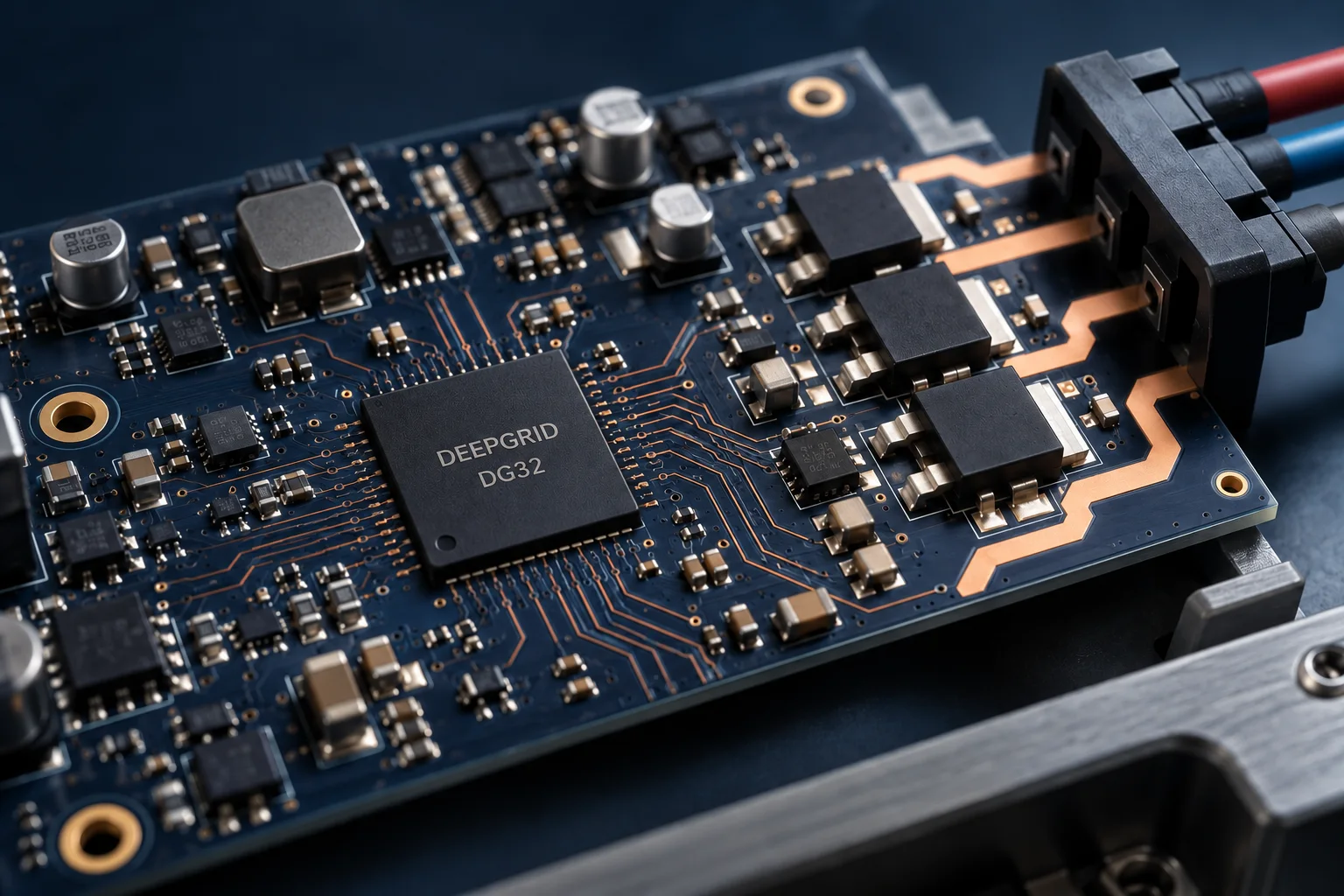
Two RISC-V cores run two cycles apart. A comparator checks every committed store, latches the first cause and drives FAULT_N, which can switch off the motor bridge without waiting for firmware: 39 cycles in simulation.
DG32 control and hardware safety. New DeepGrid product concept · concept illustration, not a product photograph or deployment evidence. DeepGrid silicon remains pre-silicon.
Two chips, one frozen safety core · 0:47, narrated. Lockstep, the fault path, timing closure and the control-loop budget. Each figure carries its basis on screen: simulated, post-route or analytic. Concept animation; DeepGrid silicon remains pre-silicon.
DG32-LITE runs a second identical core two cycles behind the first, so a datapath fault reaches the gate driver without firmware.
DG32-LITE combines a RISC-V microcontroller, the peripherals a brushless drive needs and a hardware safety monitor on one 130 nm die. The monitor is a second, identical core that runs two cycles behind the first. If the two ever disagree, the chip latches the first cause and drives a pin that can turn the power bridge off without waiting for firmware.
Six block groups share one deterministic bus on a single 50 MHz clock. Below: the four constraints that shaped the chip, then the full diagram, every block and why it exists, and how a control loop, a boot and a fault move through it.
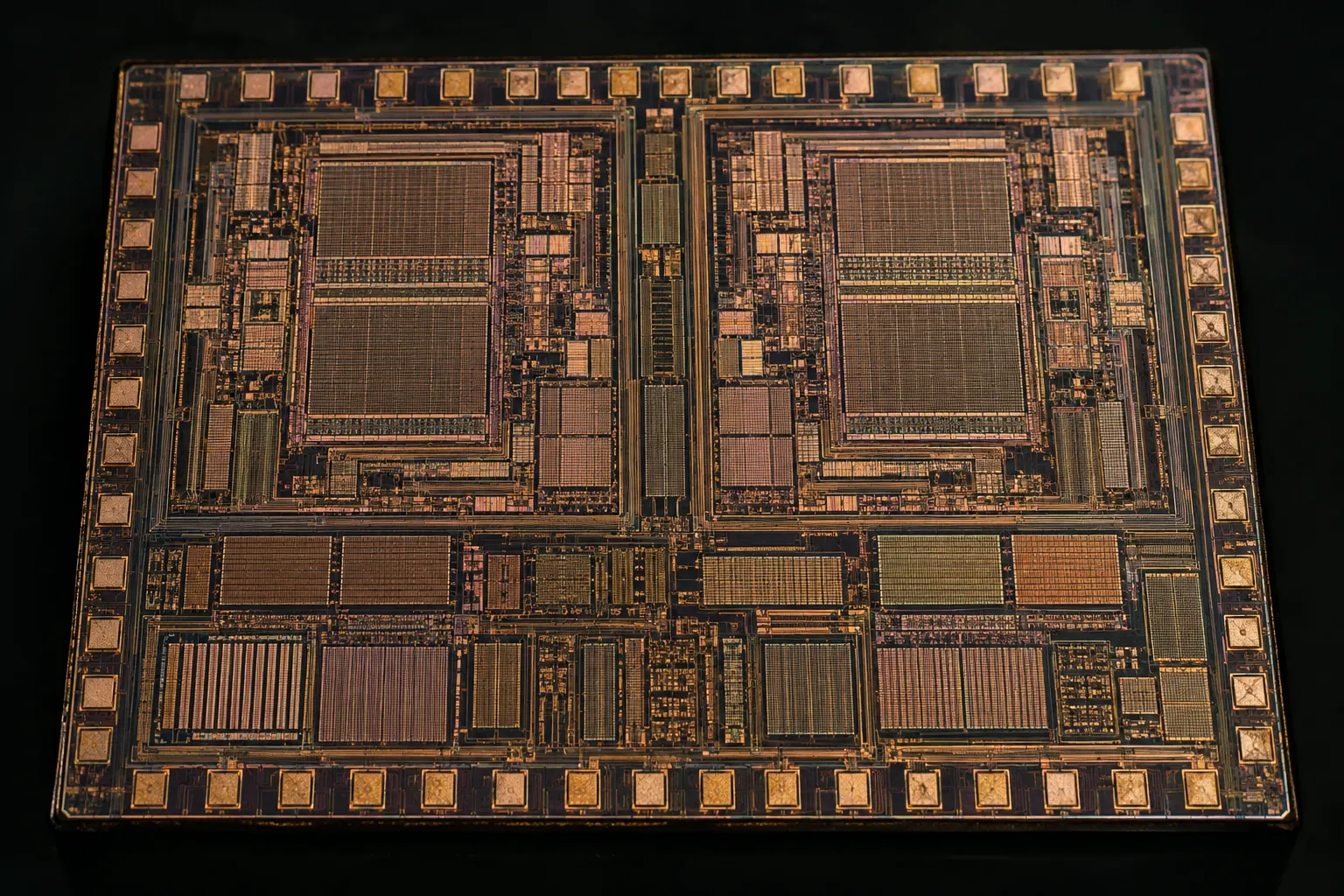
Illustration of a lockstep die: two identical cores side by side, a comparator between them. DG32’s own block diagram is below.
ONE CLOCK DOMAIN50 MHz
BUS MASTERS2
INTERRUPT SOURCES16
BOOT ROM64 KB
DUAL-PORT SRAM32 KB
FAULT TO LATCH, SIMULATED39 cycles
Four hardening findings set the shape of every block, starting with a lockstep core that tops out near 55–62 MHz.
Each constraint below sets a boundary for the customer workload and the scope of an evaluation.
Design premises and what they set
Constraint
What it means
What the design does
No debugger halt on the die
Nothing outside the chip can stop or inspect a hung CPU, and there is no management core to rescue it.
Every bad access returns a bus error instead of hanging; blank flash starts a UART monitor; the watchdog catches hangs and runaways.
Lockstep core fmax ~55–62 MHz
The CPU pair is the slowest block on the die; every peripheral hardens above 90 MHz.
The whole die runs one 50 MHz clock domain, with margin under the core’s ceiling.
~8 clock cycles per instruction
The core fetches every instruction over the bus, so control maths in plain C is slow: an int8 multiply-accumulate took 54 cycles, not the ~6 a cached core gives.
Sampling, the Park transforms and PWM edges move into dedicated blocks; the CPU keeps only the PI regulators.
Memory macros have no spare bits
There is no room for parity or ECC in the 130 nm SRAM macros.
The chip ships without memory ECC and says so. The idle second read port becomes a feed for a DMA or accelerator.
Numbered markers trace one current-control loop: ① the PWM fires the ADC sample, ② phase current goes to the CORDIC, ③ the transforms go to the CPU, ④ the PI output sets the PWM duty, ⑤ gate signals leave for the gate driver. F marks the fault latch, whose FAULT_N trips the bridge in hardware.
Control, clock and fault-path responsibilities
Numbered markers
①Marker ①: The PWM period centre fires the ADC sample, where current ripple is lowest.
②Marker ②: Phase current goes to the CORDIC, which runs the Clarke and Park transforms with the rotor angle.
③Marker ③: The transformed currents go to the CPU, which runs the d and q PI regulators in plain C.
④Marker ④: The PI output sets the PWM duty in shadow registers that load at the next period boundary.
⑤Marker ⑤: Gate signals leave for the external gate driver.
FMarker F: FAULT_N from the fault latch turns the bridge off in hardware, without firmware.
Block responsibilities
Safety core
MAIN runs the application. CHECKER runs the same instructions two cycles later on identical inputs, the comparator checks every committed store, and the fault latch holds the first cause and drives FAULT_N.
Why A silent datapath fault produces a wrong PWM edge, and a wrong edge can destroy a bridge.
The 64 KB mask ROM validates the flash image, copies it into 32 KB of dual-port SRAM and jumps to it. One SRAM port serves data, the other instruction fetch.
Why The die has no management core and no debugger halt, so the boot path must start the chip on its own.
Two masters, the CPU first and the DMA second, with single-outstanding, deterministic latency. An unmapped or disabled address completes with a bus error.
Why On a chip with no debugger, a hung bus would be a brick.
Centre-aligned complementary PWM on six gate pins with dead-time, and a hardware brake that forces all six outputs off within two clock cycles. Four DShot channels share the PWM pads.
Why Gate timing and the safe state are too important to leave to a firmware loop.
Encoder and Hall decode with edge timestamps, an 8-bit differential SAR ADC fired by the PWM, and a CORDIC for sin, cos and atan2 at a fixed cost per operation.
Why The CPU core is fetch-bound at about 8 cycles per instruction, so the expensive parts of the loop are hardware.
Background reading explains the general technique each block uses. None of it describes this part or implies its certification.
Six block groups share one deterministic 50 MHz bus, and each exists because something on the die could not be left to firmware.
Select a group to highlight it on the illustrative die and read what every block inside it does, and why it was built that way.
DG32-LITE / FUNCTIONAL BLOCK ARCHITECTURE
DRAG TO ROTATE · NOT A MASK LAYOUT
Safety core
Motor control drives power electronics. A silent CPU fault can destroy a bridge; a second core that must agree bit-for-bit turns that fault into an observable signal.
Lockstep CPU pair
MAIN runs the application; CHECKER runs the same instructions two cycles later on mirrored inputs and bus responses.
WHYTwo cores that must agree bit for bit turn a silent datapath fault into an observable one. Mirroring the bus responses means firmware can branch on peripheral reads without the cores diverging.
Comparator and fault latch
Compares every committed store; the first mismatch sets a sticky latch with its cause and drives FAULT_N.
WHYComparing on the store gives a signature that does not depend on external timing, and the first cause is the diagnostic one. A locked injection register lets firmware fire the path on purpose, the only way to prove it on real silicon.
Supervisor and windowed watchdog
Two supply-good inputs with deglitching and reset sequencing, plus a watchdog that faults on a kick that is too early or too late.
WHYA window catches runaway code as well as a hang. It arms only when firmware enables it, so it can never hold the chip in reset on a cold boot.
The 3D model is illustrative: region placement indicates grouping, not the fabricated floorplan.
One current loop costs about 300 hardware cycles at any loop rate, the boot has no rescue path, and the fault path never waits for firmware.
Three sequences explain most of the chip: the current loop it exists to run, the boot it performs on its own, and what happens when the two cores disagree.
One current-control loop
About 300 hardware cycles, the same at every loop rate.
01
Sample trigger
The PWM period centre fires the ADC, where current ripple is lowest.
02
Convert
The SAR ADC converts the phase current: 177 cycles.
03
Transform
CORDIC runs the Clarke/Park transform with the encoder angle: 53–58 cycles per operation.
04
Regulate
The CPU runs the d and q PI regulators in plain C at ~8 cycles per instruction.
05
Rotate back
CORDIC runs the inverse Park rotation.
06
Update
New duty cycles load into the PWM shadow registers at the next period boundary.
Power-on boot
No management core and no debugger: the ROM is the whole path.
01
Banner
The ROM prints a boot banner on UART0.
02
Validate
It reads and checks the image header in external QSPI flash.
03
Load
It copies the application into SRAM.
04
Run
It jumps to SRAM; the application installs its trap handler and enables interrupts.
05
Fallback
With no valid image, a UART monitor starts so a bare board can still be read, written and started.
A CPU fault
From a wrong value to a safe bridge, without firmware.
01
A datapath fault
A transient or permanent error changes a value the MAIN core is about to commit.
02
CHECKER disagrees
CHECKER runs the same instructions two cycles later on mirrored inputs and bus responses, so it commits the correct value.
03
The comparator flags it
Every committed store is compared. The first mismatch is caught on that store, not at the next software self-test.
04
The first cause is latched
A sticky fault latch holds the first cause, because later faults are usually its consequences. Firmware can read it after the fact.
05
The bridge turns off
FAULT_N goes low within 39 cycles of an injected fault in simulation. Wired to the gate-driver enable, it stops the bridge without waiting for firmware.
Four decisions are frozen until first-silicon test, and the largest is that the control core will not be reopened for features.
These are settled. Each trades something away on purpose, and the reason is recorded with it.
Freeze the control core
The lockstep pair, its boot path and the bus decode are closed until silicon test.
WHYIt is hardened, gate-level clean and simulated end to end. Reopening it for features risks the one part that must be right on a shuttle with no respin.
Give fetch its own path
Instruction fetch reads a private boot ROM and SRAM port; the shared bus carries only data.
WHYSeparating fetch from data traffic removes a whole class of arbitration bugs instead of patching them, and data traffic can never stall execution.
Error slave, not dead decode
Unmapped or clock-gated addresses complete with a bus error.
WHYWith no debugger and no halt, a hung bus would brick the chip. Firmware has to see a bad access and survive it.
Share the motor pads
DShot is multiplexed onto the PWM output pads and selected at boot.
WHYAn output is either a complementary PWM leg or a DShot line, never both. Duplicating pads would spend package pins for no added capability.
The lockstep core is the slowest block, so it sets the clock.
Maximum frequency of each hardened block after place-and-route. Every peripheral clears 90 MHz; the lockstep core reaches ~55–62 MHz, which is why the die runs at 50 MHz. The same limit is why DG32-2DOM puts its engine on a second clock instead of raising this one.
Post-route maximum frequency by block, in MHz
GPIO
GPIO · 173.6 MHz
173.6
DShot
DShot · 172.9 MHz
172.9
QSPI controller
QSPI controller · 171.6 MHz
171.6
PWM
PWM · 167.8 MHz
167.8
Lockstep checker
Lockstep checker · 123.6 MHz
123.6
CORDIC
CORDIC · 95.5 MHz
95.5
Supervisor
Supervisor · 91.1 MHz
91.1
Lockstep core
Lockstep core · 55–62 MHz
55–62
50 MHz target
0180 MHz
Post-route figures on the 130 nm process. The lockstep-core bar is drawn at 55 MHz, the low end of its measured range.
Pre-silicon. Figures are design values verified in simulation and static timing, not measurements on fabricated parts, unless marked otherwise.